

N1 Carrier 3 - FPV
R0033Rev B.0Active
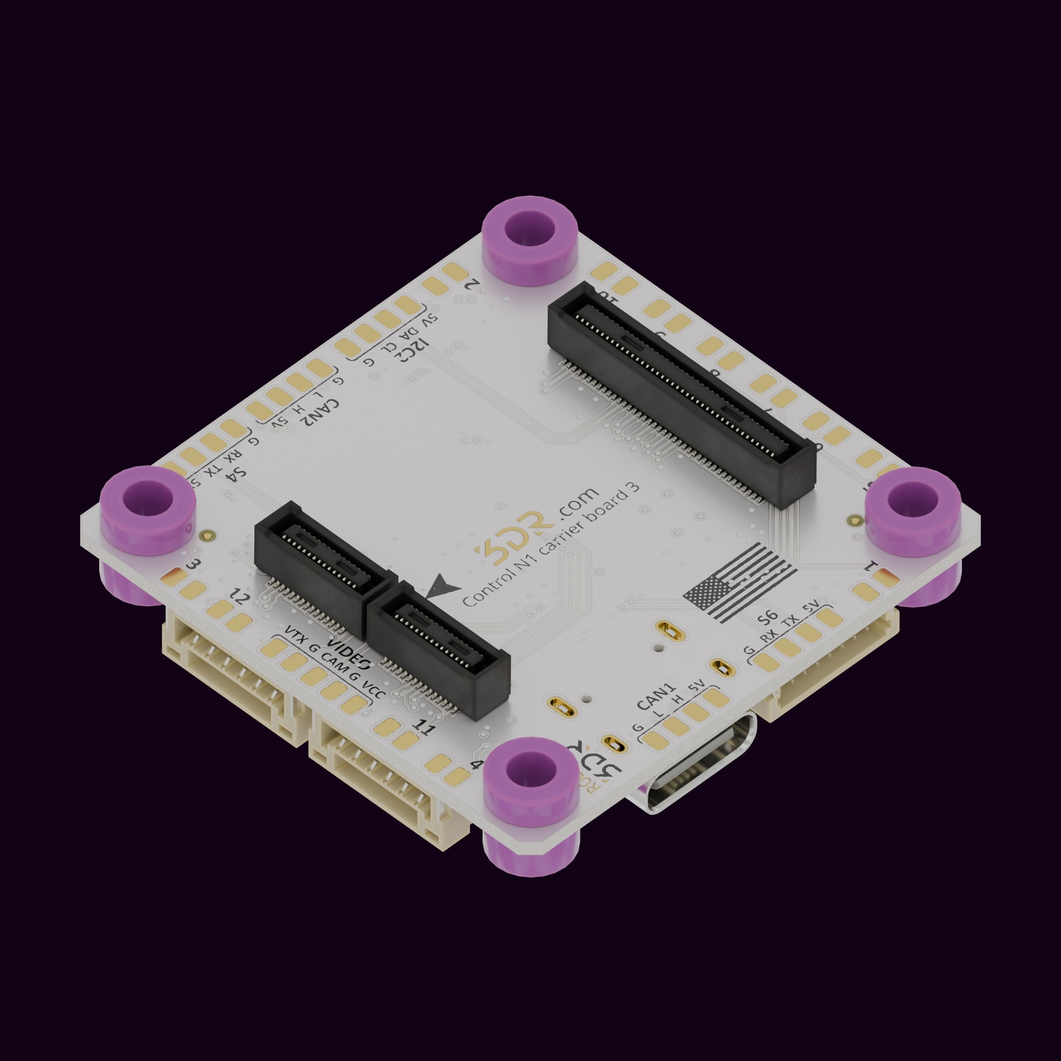
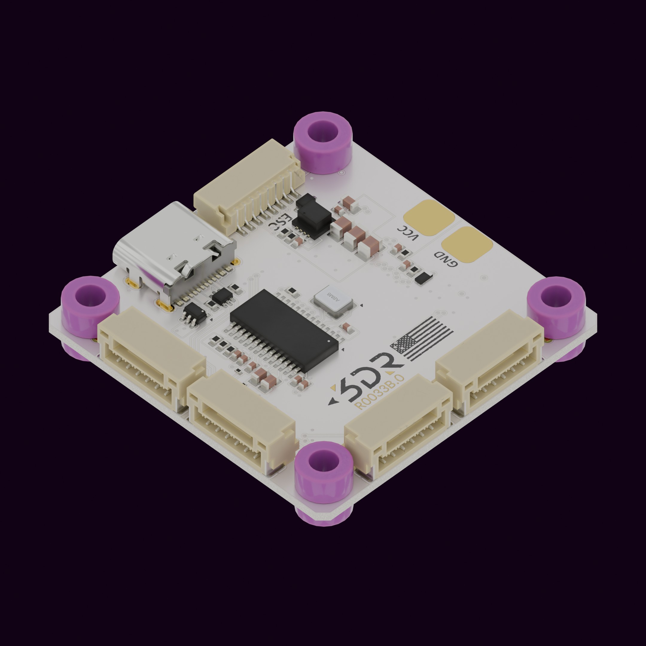
The Carrier Board 3 for the Control N1 (R0033) is designed for FPV platforms. It follows a universal mounting standard that fits most FPV and DIY drone frames, sized to work with standard 4-in-1 ESC + Power Distribution Board stacks. The 8-pin JST connects directly to 4-in-1 ESC boards for easy integration and less wiring complexity. The onboard OSD outputs flight data (battery voltage, altitude, speed, distance, coordinates) to analog video transmitters.
Specifications
Section titled “Specifications”| Specifications | 3DR N1 Carrier 3 - FPV (R0033) |
|---|---|
| Mounting Holes | M3, 30.5 mm x 30.5 mm |
| Weight | 6.5g alone 9.2g with N1 |
| Dimensions | See Mechanical Information |
Electrical
Section titled “Electrical”| Electrical Specifications | 3DR N1 Carrier 3 - FPV (R0033) |
|---|---|
| Operating voltage | 6.4V - 36V |
| Battery input | 3S - 8S |
| Peripheral output voltage | 5V |
Available Ports
Section titled “Available Ports”| Port | Connection Type |
|---|---|
| USB | USB-C |
| VBATT | Pads |
| GPS1 (SG7 + I2C1) | JST-GH |
| Serial 1 (SG1) w/Flow Control | JST-GH |
| Serial 2 (SG2) w/Flow Control | JST-GH |
| Serial 3 (SG3) w/Flow Control | JST-GH |
| Serial 4 (SG4) | Pads |
| Serial 6 (SG6) | Pads |
| I2C2 | Pads |
| CAN1 | Pads |
| CAN2 | Pads |
| Video | Pads |
| PWM Channels 1-12 | Pads |
| ESC (uses PWM channels 1–4) | JST-SH |
3D View
Section titled “3D View”Loading 3D model…
Installation & Setup
Section titled “Installation & Setup”- Unpack the product and inspect for any visible damage.
- Align the connector/interface with the corresponding port on Control N1 (R0024).
- Secure the connection by pressing firm and equally both boards against each other.
- Power On the base product to verify successful integration.
Connector Pinouts
Section titled “Connector Pinouts”
60%
| Pin | Signal | Description |
|---|---|---|
| 1 | VCC | Battery supply |
| 2 | GND | Ground |
| 3 | CH1 | PWM |
| 4 | CH2 | PWM |
| 5 | CH3 | PWM |
| 6 | CH4 | PWM |
| 7 | NC | Not Connected |
| 8 | NC | Not Connected |
| Pin | Signal | Description |
|---|---|---|
| 1 | 5V | 5V input for GPS |
| 2 | S7_TX | Serial transmit from GPS |
| 3 | S7_RX | Serial receive to GPS |
| 4 | I2C_SCL | I2C clock line |
| 5 | I2C_SDA | I2C data line |
| 6 | GND | Ground |
| Pin | Signal | Description |
|---|---|---|
| 1 | +5V | +5V power input |
| 2 | S(1,2,3)_TX | Serial transmit (UART TX) |
| 3 | S(1,2,3)_RX | Serial receive (UART RX) |
| 4 | S(1,2,3)_CTS | Clear To Send (hardware flow control) |
| 5 | S(1,2,3)_RTS | Request To Send (hardware flow control) |
| 6 | GND | Ground |
All pads are labeled on the board itself.
Mechanical Information
Section titled “Mechanical Information”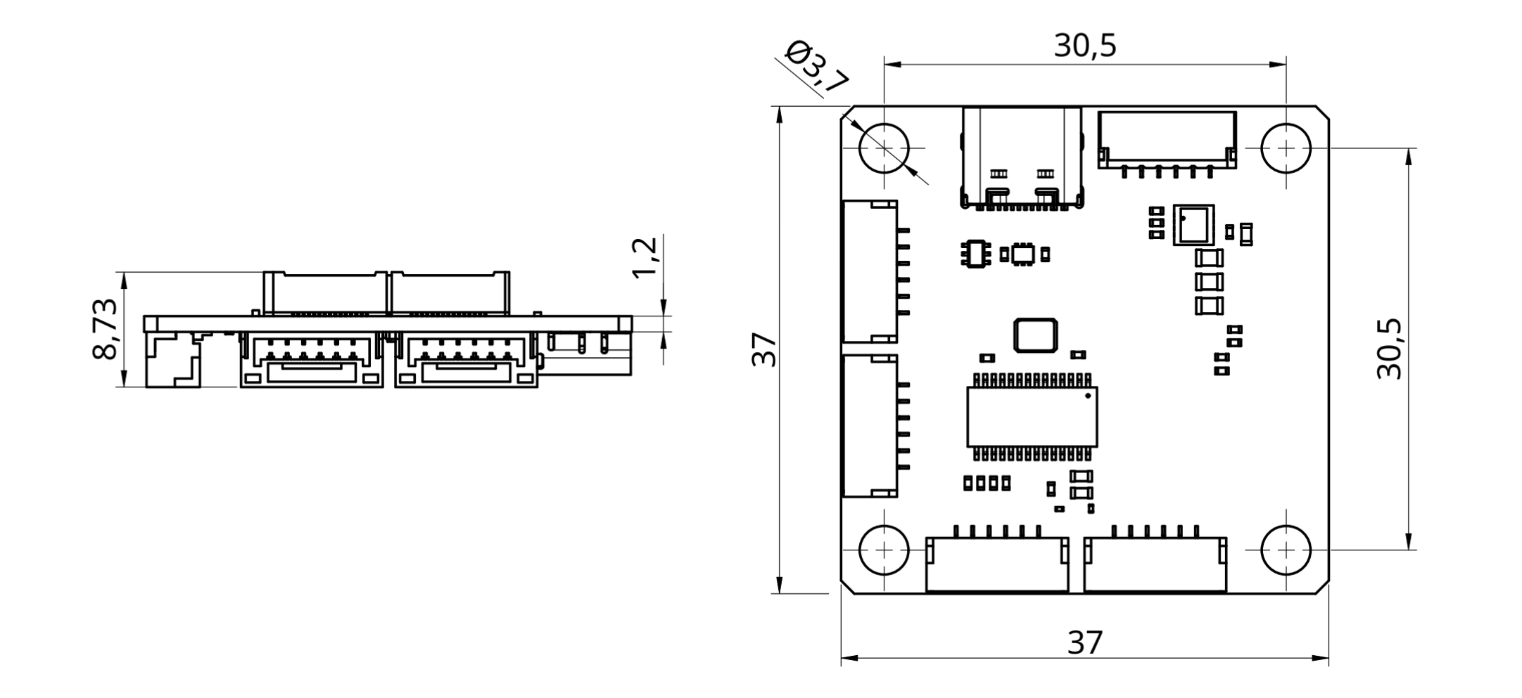
Stack height with N1 mounted: 10.0mm
Power Distribution
Section titled “Power Distribution”Do not use both power inputs simultaneously — use only one at a time.
Changelog
Section titled “Changelog”Rev A.1 - 4S max input voltage only (16.8V).
- The input protection diode above the ESC connector on the bottom side can be removed to allow up to 8S, but this is not recommended as it could damage the board.
Maintenance
Section titled “Maintenance”- Clean with a dry cloth; avoid moisture or abrasive materials.
- Periodically check connection points for wear or loosening.
- Store in a cool, dry place when not in use.
If you have further questions, contact us.
Downloads
Section titled “Downloads”R0033 STEP File